
SVT Associates is a world
leading manufacturer of
Molecular Beam Epitaxy
systems and other Thin
Film Deposition Equipment.

leading manufacturer of
Molecular Beam Epitaxy
systems and other Thin
Film Deposition Equipment.
Application Laboratory & Wafer Services


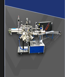
SVT Associates, Inc. has been actively working on the growth and characterization of III-Nitride materials and devices since 1992 using RF atomic nitrogen plasma assisted molecular beam epitaxy (PA-MBE). Wafer growth and characterization services are explained below:
III-Nitride MBE Wafer Specifications:
|
GaN, AlGaN, InGaN |
|
<2% |
|
<3 arc min |
|
1017 to 1020 cm-3 |
|
up to 1019 cm-3 |
|
Nd <1016 cm-3 |
|
>1500 cm2 /Vs (300K) |
| >4000 cm2 /Vs (77K) | |
|
Sapphire, SiC, Si |
* HEMT characteristics depend on buffer and active layer structure.
III-Nitride Epitaxial Services:
- Nitride MBE growth on sapphire and silicon-carbide 2" and 3" wafers:
- GaN (n-type, p-type, or insulating)
- Custom ternary & quaternary InAlGaN films
- High-frequency, high-power and low-noise III-N transistors:
- High electron mobility transistors (HEMTs)
- Bipolar junction transistors (HBTs & BJTs)
- AlxGa1-xN high-efficiency, solar-blind UV photodetectors (PD):
- Schottky and p-i-n PDs with cutoff wavelength from 365 down to 250 nm
- Special structures including arrays, bandpass and MQW detectors
- Custom epitaxial layers and structures, including:
- Doped and undoped superlattice structures
- Resonant tunneling structures (RTDs)
- Wafer characterization:
- In-situ cathodoluminescence
- AFM and X-ray characterization
- CV and Hall measurements
Contact SVTA for more information.